Outstanding Arm-ECS graduate claims Young Engineer of the Year accolade
18th August 2021
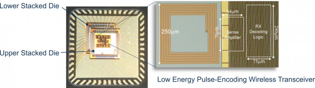
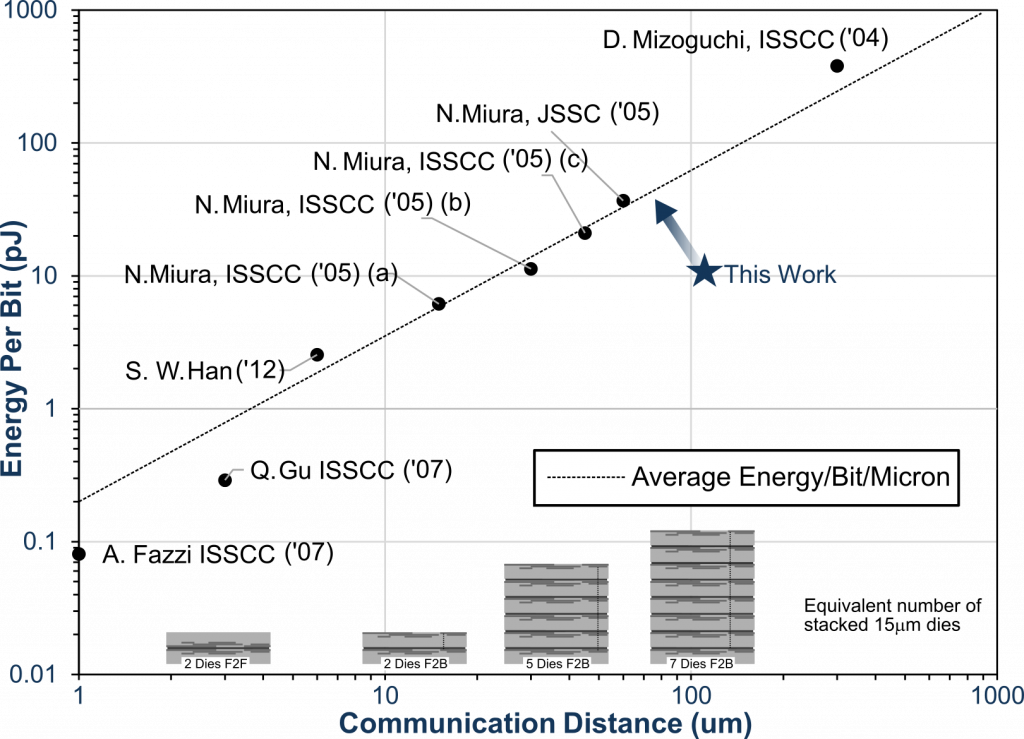
Former University of Southampton postgraduate research student Ben Fletcher has been named as a winner of the Royal Academy of Engineering (RAEng) Engineers Trust Young Engineer of the Year competition. The electronic engineer is recognised for outstanding success in his early career, having advanced novel approaches for cost-effective three-dimensional integrated…