Making Stacking Silicon as Easy as Stacking Lego (2/2)
Wireless 3D Integration – Making Stacking Silicon as Easy as Stacking Lego (2/2)
This blog post originally appeared on https://community.arm.com
In the previous instalment of this blog series we discussed some of the benefits that contactless (or wireless) 3D integration can offer in an Internet of Things (IoT) context. These being: low cost manufacturing and assembly, short design cycles, facility for heterogeneous integration, and intrinsic voltage level conversion. But how are they designed? In this second instalment, we dive into the technical details of how these wireless inter-tier links can be realised. Summarising some of the recent research contributions from the Arm-ECS Research Centre including COIL-3D (our automated CAD tool for the generation of ICL inductors). Our award-winning low energy data transceiver (using spike-based time-domain encoding), and finally CoDAPT (our wireless transceiver for Concurrent Data and Power Transmission).
Inductive Coupling Links
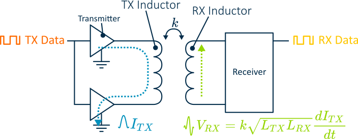
Figure 3 – Schematic illustration of a wireless inductive coupling link and fundamental equations showing operation.
As discussed in the previous instalment, inductive coupling links are a form of near-field communication that relies on Faraday’s principle of electromagnetic induction. The link consists of two inductors (one transmitting, TX, inductor, and one receiving, RX, inductor) as shown in the figure above.
To transmit data wirelessly through the 3D stack, it is encoded as a series of current pulses which are fed through the TX inductor, as shown by ITX in the figure. This results in a magnetic field being formed within the die stack, that will get intersected by similar planar inductors in each receiving die. Through electromagnetic induction, this intersection causes a voltage VRX to appear at the receiver. This is given by the equation shown in Figure 3 – a combination of LTX, LRX (the inductances of the TX/RX inductors), ITX and k which is the channel coupling coefficient.
As can be immediately observed from this equation, the channel coupling coefficient, k, is an important factor that needs to be maximised to ensure the link operates with the highest efficiency. There are many variables that affect the channel coupling coefficient. However, the most notable are the physical layout parameters of the inductors used for forming the channel, for example the size, shape, track width, track spacing, number of turns, etc.
The relationship between these physical parameters and the electrical coupling performance of the channel is not straightforward. And, to translate one to the other typically requires a 3D model of the inductor to be created, and then converted into a mesh which can analysed using specialist finite element modelling (FEM) software. This is not a simple process and can take many hours, even just for analysing a single inductor. One of the first outputs of our research at the Arm-ECS Research Centre addresses this design challenge directly. We have developed ‘COIL-3D’, a handy software tool for completely automating the design and optimisation process for inductors used in wireless 3D-ICs.
COIL-3D – Automated Layout Generation for ICL Inductors
COIL-3D (a CAD-tool for the Optimisation of Inductive Links in 3D-ICs) completely automates the process of selecting the best physical layout parameters for the inductors used in wireless 3D-ICs. Figure 4 shows conceptually the operation of the COIL-3D tool. Starting with an input specification, the COIL-3D tool generates
- (1) an optimised inductor layout to maximise channel coupling depending upon your input specification.
- (2) a SPICE model of the optimised inductive channel that can be used to simulate the design with conventional commercial circuit simulators.
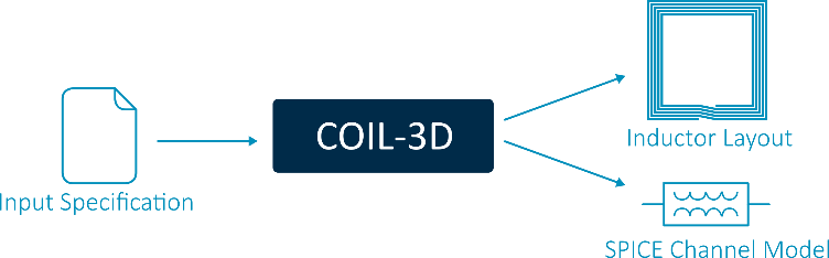
Figure 4 – Conceptual illustration of the COIL-3D use case
Because of the slow nature of finite element modelling (FEM), it would be practically impossible to simulate all the possible different design permutations for a given wireless 3D chip using it. In fact, the ‘back-of-the-envelope’ calculations presented in our paper suggest it would take over 500 years to do these simulations! Therefore, to address this issue in COIL-3D, we use a different approach. We break the inductor down into a combination of multiple individual segments, as shown in Figure 5. A set of strictly solvable mathematical expressions are then used to evaluate: the resistance of each segment (R). The inductance of each segment (L), the capacitance between segments (C), and the mutual inductance between segments (M) directly from the physical layout parameters. These can then be combined together to generate an approximate model as shown below.
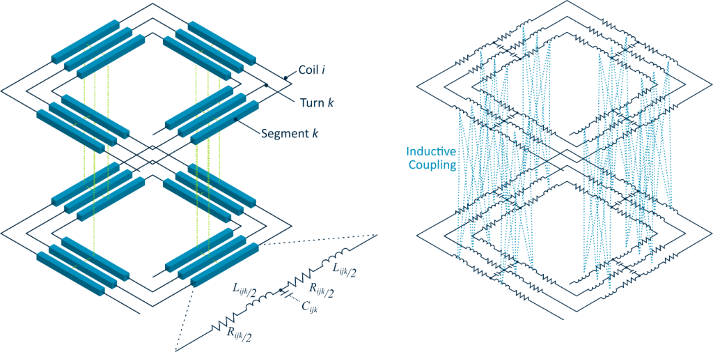
Figure 5 – Scalable ‘segmented’ inductor model developed for use in COIL-3D.
Using our approximate model, the COIL-3D tool can analyse a given set of layout parameters within around 80ms. Whilst the results may not be quite as accurate as using FEM, our expressions are pretty good and achieve an average accuracy within 7.8% of the commercial finite element modelling software tools. COIL-3D combines this speedy evaluation approach with a refined optimisation flow that finds the best parameters for your design in less than one hour. This allows designers to start with the most power efficient inductive link design for their given integration scenario.
To read more about COIL-3D, or to download the code to use it for your project, please take a look at our publications in IEEE Transactions on VLSI or the Design Automation and Test in Europe (DATE) conference, 2017.
A Low Energy Data Transceiver
Aside from optimising the physical design of the inductive link, another of our research focuses has been exploring how the data can be encoded in the transceiver, to reduce power consumption (and hence maximise the battery life of the devices which they end up in, as much as possible). One intuitive way of designing a link is to send one current pulse for every transmitted bit, perhaps changing its polarity depending on the value (for example a positive pulse for representing a ‘1’ and a negative pulse for representing a ‘0’). Whilst this is a valid solution to the transceiver design problem, it requires sending as many pulses as there are data bits, which quickly burns lots of power.
To address this challenge, we have designed a novel transceiver that uses spike-latency encoding (also known as pulse-position modulation). In this spike-latency transceiver, multiple (N) bits are encoded with a single current pulse by using the delay with which it is transmitted to represent the data. This may sound confusing at first, however the concept is relatively simple, and illustrated by the figure below.
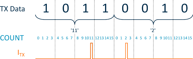
Figure 6 – Illustration showing the operation of our proposed spike-latency encoding transceiver.
Here N bits (in this case N=4) are encoded using a single pulse with a delay corresponding to their value. For example, the first four binary bits are 1011 (‘11’ in decimal). Therefore, a pulse is sent when the internal counter reaches 11. Similarly, for the data pattern 0010, a pulse is sent when the internal counter reaches 2. If the counters in each stacked die (transmitting and receiving) are synchronised, this approach allows the energy consumption to be reduced significantly.
This spike-latency transceiver was recently presented at the International Symposium on Low Power Electronics and Design 2019, where it won the ‘Best Paper’ award, and since then has been implemented in the first of our silicon showcase chips (shown in Figure 7).
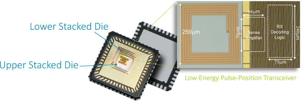
Figure 7 – Photograph showing our first wireless 3D silicon test chip, highlighting the proposed low energy transceiver.
Test chip measurements show impressive energy reductions, with the full transceiver consuming only 10.8pJ/bit. This represents a 30% energy reduction compared to state-of-the-art transceivers when considering the communication distance, as shown in Figure 8 below.
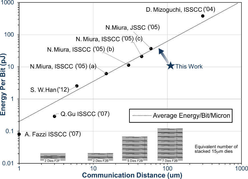
Figure 8 – Energy-per-bit-per-communication distance of our spike-latency encoding transceiver when compared to other state-of-the-art transceivers.
More details about the transceiver design and silicon test chip measurements will be presented at the European Solid State Circuits conference 2019 later this month.
Wireless Power and Data Delivery
The final research strand that we have been exploring at the Arm-ECS Research Centre is wireless power delivery. Whilst the wireless schemes discussed above offer a great way of communicating data between stacked silicon tiers, each of these stacked silicon dies must also have a power source.
We have been researching ways of combining wireless data transfer (as discussed above) and wireless power transfer (like that used in your everyday wireless phone chargers, or even rechargeable toothbrushes) within the same link for use in 3D-ICs. To achieve this, we have developed a new transceiver architecture CoDAPT, for Concurrent Power and Data Transfer, which is shown in Figure 9 below.
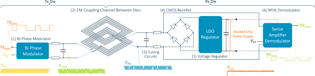
Figure 9 – Schematic diagram showing the architecture of a Concurrent Data and Power Transfer (CoDAPT) link.
In a CoDAPT link, instead of using a pulse-based modulation scheme for encoding the data (as we discussed previously in the post). We use Bi-Phase Shift Keying (BPSK) modulation where the high-frequency carrier signal is used to deliver power wirelessly. Whilst the data is communicated by means of phase encoding (inverting the carrier signal at every data edge) (as shown in part (1) of Figure 9).
To make the link operate with maximum efficiency, we also tune the system such that the carrier signal frequency matches the resonant frequency of the inductive link (shown in part (3) of Figure 9). On the receiver side, the high frequency signal can then be rectified and regulated to use as a power source (shown in part (4) and part (5) of Figure 9), and its phase can be periodically sampled to recover the transmitted data. This provides an ‘all-in-one’ interface for wireless 3D integration where power and data are both provided through a single link.
Simulation results from the proposed CoDAPT link, presented at Design Automation and Test in Europe (DATE) 2019, show that we can achieve a data rate of 1.3Gbps (BER< 10−9) whilst simultaneously transferring up to 2.1mW of power per channel. The CoDAPT link has also been successfully implemented on our second wireless 3D silicon test-chip, and test results from real silicon measurements will be published very soon.
To summarize, 3D integration is set to be a key enabling technology in the Internet-of-Things era, but the cost of manufacturing heterogeneous 3D stacks using TSVs is prohibitively expensive for IoT applications. At Arm Research we have been exploring one alternative to this which is wireless 3D integration using near-field inductive coupling links. This post has outlined 3 of our most recent research outputs: COIL-3D, our low energy spike-latency encoding transceiver, and CoDAPT (our wireless transceiver for Concurrent Power and Data Transmission), however there is still much more research going on. If you are interested in learning more about any of these three topics, or have any questions about our wireless 3D integration research in general, please check out our papers, or feel free reach out directly.