Making Stacking Silicon as Easy as Stacking Lego (1/2)
Wireless 3D Integration – Making Stacking Silicon as Easy as Stacking Lego (1/2)
This blog post originally appeared on https://community.arm.com
Over the past few years, the growth of the Internet of Things (IoT) has brought about a range of new challenges for IC designers. IoT devices are required to perform a range of different functions. These range from; analogue sensing and energy-harvesting, to digital processing and wireless communication), all within very strict power and volume constraints. To manage this, it is becoming commonplace that integration of these different components happens within the chip. Often, however, each component requires its own silicon process technology, so combining these different elements is not a straightforward task.
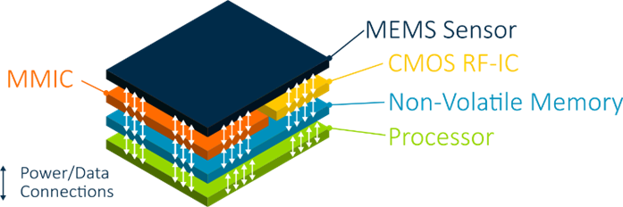
Figure 1 – Illustration of a hypothetical heterogeneous 3D stacked IC system.
One solution to this challenge is fabricate each die in its own process technology, and then stack them up. This is known as ‘3D integration’. Figure 1 shows an example of such a 3D stacked IC. The design of each of the stacked tiers is understood. In addition, to physically build this chip, a way of communicating the data vertically through the system (as illustrated by the arrows in Figure 1) is also required.
To do this, most of the research community are focusing on the development of through silicon vias (TSVs). TSVs are metal pillars, etched entirely through each silicon die, to provide electrical connectivity with neighbouring tiers. TSVs promise high density, high bandwidth communication and are already being deployed in some high-end commercial memory stacking applications. However, designing with TVSs is expensive. The fabrication and assembly processes used in TSV-based 3D-IC manufacture are only available in the very latest technology nodes. These vary from foundry to foundry. IoT devices are supposed to be ubiquitous, low-cost and disposable. This makes incorporating the high-cost technology unfeasible.
Our latest research is looking into a novel, low-cost alternative where communication between silicon layers is completely wireless. The use of wireless communication avoids the following: inflated design, manufacture and testing costs associated with TSV-based 3D integration. This makes it ideally suited to cost sensitive IoT applications. We are aiming to develop a research prototype of a standardised low-power wireless interface that vendors can include on their dies. This will allow designers to pick and choose a set of circuit blocks and stack them up with no additional fabrication processing, just like building with Lego!
How does Wireless 3D Integration Work?
To maintain good energy efficiency, wireless 3D integration usually operates using near-field region of the electromagnetic spectrum, more specifically using inductive coupling. But, how does this work? When using inductive coupling to communicate data between tiers within the 3D stack, data is encoded as a series of current pulses. These current pulses are then fed through a planar metal inductor, fabricated in the transmitting die. This forms a magnetic field within the 3D stack (as shown in Figure 2 (b)). These can be sensed by similar inductors fabricated in each of the receiving (RX) dies (through electromagnetic induction) and then used to decode the transmitted data stream. This inductive communication technology is very similar to that used in your contactless payment cards, but shrunk right down to fit within a silicon chip (in fact, the transceivers in our latest test-chip are as small as 150um in diameter – about 2-3x the width of a human hair).
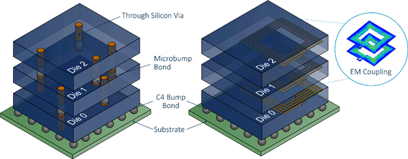
Figure 2 – A comparison of a stacked 3D-IC assembled using TSVs (left) and wireless inductive coupling links (right).
The image above compares 3D stacking using through silicon vias on the left, with inductive coupling links on the right. Note the need for precise micro-bump bonding between tiers is avoided when using inductive links and instead, dies can be stacked using glue, simplifying the assembly process significantly.
Going Wireless: What are the Benefits?
There are several significant benefits associated with using wireless inter-tier links in favour of TSV-based approaches. Some of these are:
- Cheap manufacturing and assembly – when using wireless links, you no longer require the expensive additional processing associated with TSV manufacture. Or, precise die-to-die stacking alignment. Instead, the wireless links can be fabricated in existing process technologies and stacked with coarse placement accuracy whilst still maintaining high reliability
- Short design cycles – another benefit is that wireless links can be designed and verified using existing 2D CAD tools; there is no need to develop/purchase additional 3D-specific EDA software
- They can be integrated at any technology node – as wireless ICLs do not require any additional fabrication processing, they can be realised at any of the existing planar technology nodes
- Intrinsic voltage level conversion – as data is communicated using electromagnetic coupling, rather than conventional electrical connections, there is no need for voltage-level conversion between stacked dies operating at different voltages. In fact, the wireless approach benefits from full electrical isolation between each of the stacked tiers
Recent Wireless 3D Research at Arm
At Arm Research (in collaboration with the University of Southampton) as part of the Arm-ECS Research Centre, we have been developing the transceiver and interface circuits to bring wireless 3D integration from concept to reality. We have already developed an openly available CAD tool (COIL-3D) for optimised design and layout of ICL inductors, and more recently we have designed a super low-energy inductive transceiver for wireless data (and even power) delivery between stacked silicon tiers.
If you are interested in learning more about the design of these systems, in the second part of this blog series – I provide a more-in-depth technical discussion covering contactless 3D-IC design, from a circuits perspective.